Patents
Patent 1: Low thermal budget dielectric stack for SONOS nonvolatile memories
Pub. No.: US 2006/00942.57 A1
Pub. Date: May 4, 2006
ABSTRACT
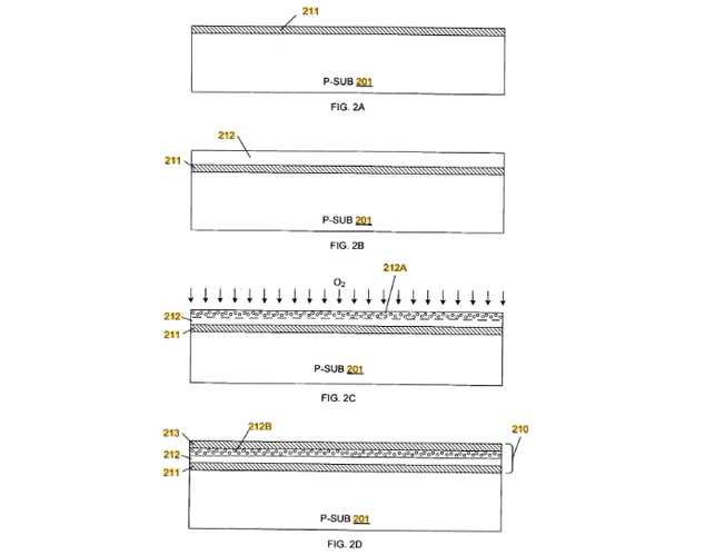
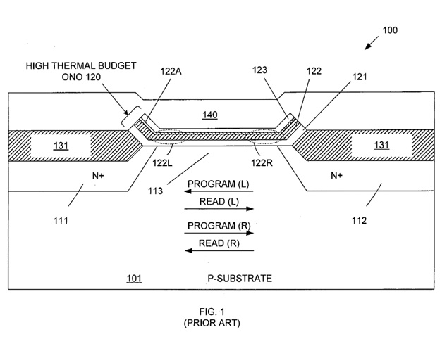
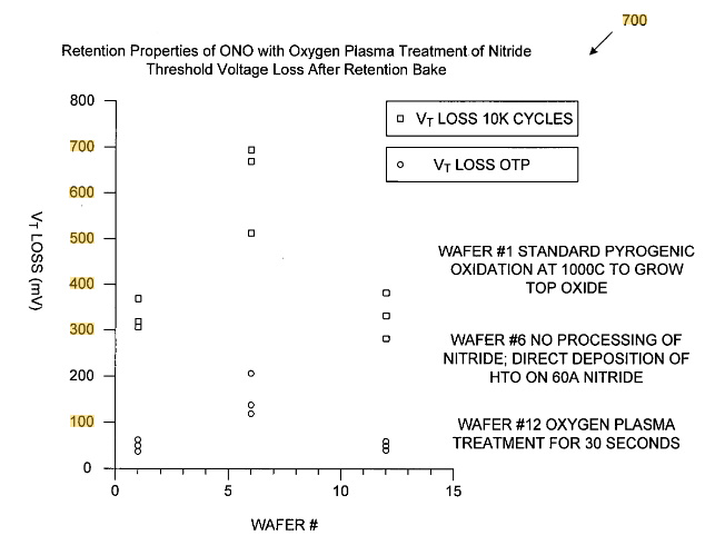
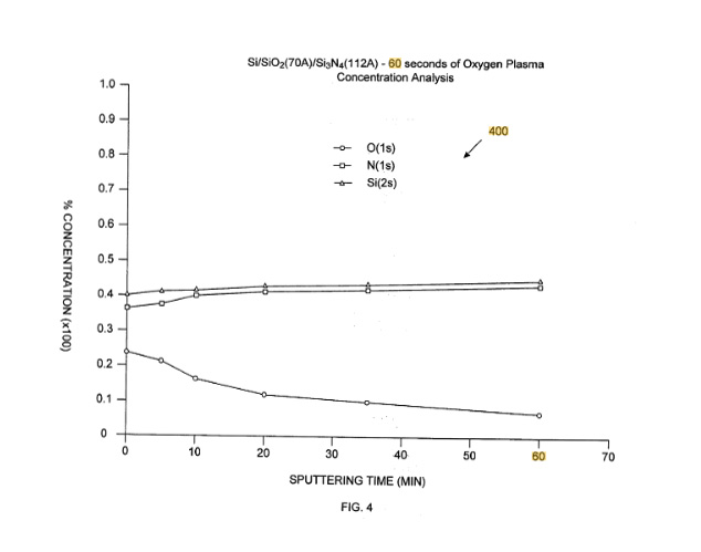
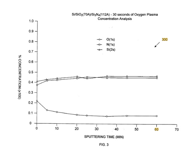
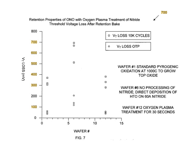
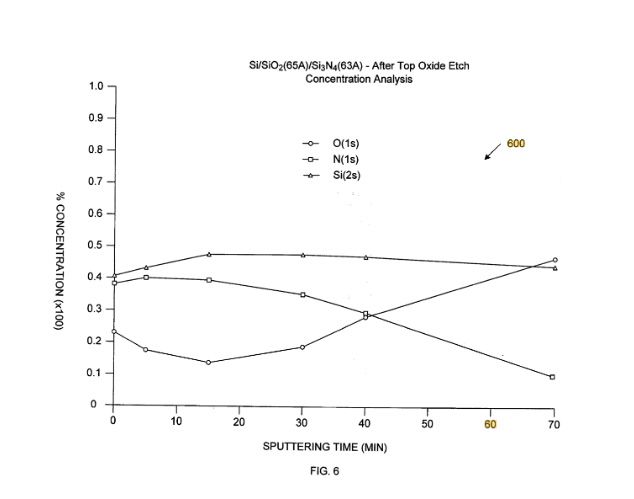
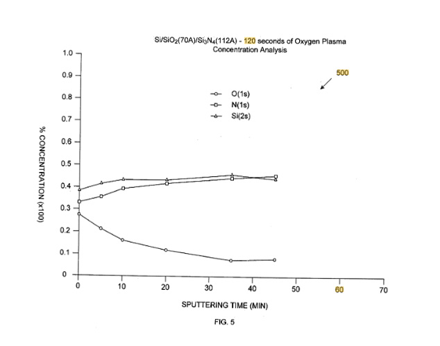
A method of forming an oxide-nitride-oxide (ONO) structure for use in a non-volatile memory cell, which includes (1) forming a first oxide layer over a substrate, (2) forming a silicon nitride layer over the first oxide layer, (3) introducing oxygen into a top interface of the silicon nitride layer, and then (4) forming a second oxide layer over the silicon nitride layer
 |  |  |
 |  |  |
 |  |  |
Patent 2: Diamond-coated substrates
Pub. No.: US 9,487,856 B2
Pub. Date: November 8, 2016
ABSTRACT
A composite structure, comprising a cemented carbide substrate (e.g., tungsten carbide substrate cemented with cobalt, such as WC—Co), a thin interlayer disposed over the substrate, and a contiguous diamond film disposed over the interlayer, as well as processes of preparing such a composite structure and uses thereof, are provided. The composite structure is characterized by at least one of a substrate binder concentration of at least 2 percents by weight, interlayer thickness less than 20 microns, a homogenous interlayer made substantially of crystalline chromium nitride, a low to null binder concentration in the interlayer, and a high co-adhesion of the diamond film to the interlayer and the interlayer to the substrate
 |  |  |
 |  |  |
 |  |  |
